(China (Mainland))


Product Summary
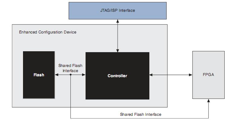
The EP20K100EQC208-2 is a single-device, high-speed, advanced configuration solution for very high-density FPGA. The EP20K100EQC208-2 is used to store configuration data for systems made up of one or more Altera FPGAs. Unused portions of the flash memory can be used to store processor code or data that can be accessed via the external flash interface after FPGA configuration is complete. The EP20K100EQC208-2 features multiple configuration schemes. In addition to supporting the traditional passive serial (PS) configuration scheme for a single device or a serial device chain, the enhanced configuration device features concurrent configuration and parallel configuration.
Parametrics
EP20K100EQC208-2 absolute maximum ratings: (1)Supply voltage:-0.2V to 4.6V; (2)DC input voltage:-0.5V to 3.6V; (3)DC VCC or ground current:100mA; (4)DC output current, per pin:-25mA to 25mA; (5)Power dissipation:360mW; (6)Storage temperature:-65℃ to 150℃; (7)Ambient temperature:-65℃ to 135℃; (8)Junction temperature:135℃.
Features
EP20K100EQC208-2 features: (1)Standard flash die and a controller die combined into single stacked chip package; (2)External flash interface supports parallel programming of flash and external processor access to unused portions of memory; (3)Page mode support for remote and local reconfiguration with up to eight configurations for the entire system ; (4)Supports byte-wide configuration mode fast passive parallel(FPP); 8-bit data output per DCLK cycle; (5)Supports true n-bit concurrent configuration (n = 1, 2, 4, and 8) of Altera FPGAs; (6)Pin-selectable 2-ms or 100-ms power-on reset (POR) time ; (7)Configuration clock supports programmable input source and frequency synthesis; (8)Supply voltage of 3.3 V (core and I/O); (9)Hardware compliant with IEEE Std. 1532 in-system programmability (ISP) specification; (10)Supports ISP via Jam Standard Test and Programming Language(STAPL); (11)Supports JTAG boundary scan; (12)nINIT_CONF pin allows private JTAG instruction to start FPGA configuration; (13)Internal pull-up resistor on nINIT_CONF always enabled; (14)User programmable weak internal pull-up resistors on nCS and OE pins; (15)Internal weak pull-up resistors on external flash interface address and control lines, bus hold on data lines; (16)Standby mode with reduced power consumption.
Diagrams
| Image | Part No | Mfg | Description |  |
Pricing (USD) |
Quantity | ||||||
|---|---|---|---|---|---|---|---|---|---|---|---|---|
 |
 EP20K100EQC208-2 |
|
IC APEX 20KE FPGA 100K 208-PQFP |
Data Sheet |
|
|
||||||
|
EP20K100EQC208-2X |
|
IC APEX 20KE FPGA 100K 208-PQFP |
Data Sheet |
|
|
||||||
|
EP20K100EQC208-2XN |
|
IC APEX 20KE FPGA 100K 208-PQFP |
Data Sheet |
|
|
||||||