Product Summary
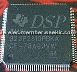
The TMS320F2810PBKA is a 150MHz Digital Signal Processor.
Parametrics
TMS320F2810PBKA absolute maximum ratings: (1)Supply voltage range:-0.3 V to 4.6 V; (2)Supply voltage range, VDD, VDD1:-0.5 V to 2.5 V; (3)VDD3VFL range:-0.3 V to 4.6 V; (4)Input voltage range, VIN :-0.3 V to 4.6 V; (5)Output voltage range, VO:-0.3 V to 4.6 V; (6)Input clamp current, IIK (VIN < 0 or VIN > VDDIO):± 20 mA; (7)Output clamp current, IOK (VO < 0 or VO > VDDIO):± 20 mA; (8)Operating ambient temperature ranges, TA: A version (GHH, PGF, PBK):-40℃ to 85℃, S version (GHH, PGF, PBK):-40℃ to 125℃, Q version (GHH, PGF, PBK):-40℃ to 125℃; (9)Storage temperature range:-65℃ to 150℃.
Features
TMS320F2810PBKA features: (1)High-Performance Static CMOS Technology:150 MHz (6.67-ns Cycle Time),Low-Power (1.8-V Core @135 MHz, 1.9-V Core @150 MHz, 3.3-V I/O) Design; (2)JTAG Boundary Scan Support; (3)16 x 16 and 32 x 32 MAC Operations; (4)16 x 16 Dual MAC; (5)Harvard Bus Architecture; (6)Atomic Operations; (7)Fast Interrupt Response and Processing; (8)Unified Memory Programming Model; (9)4M Linear Program/Data Address Reach; (10)Code-Efficient (in C/C++ and Assembly); (11)On-Chip Memory:Flash Devices: Up to 128K x 16 Flash(Four 8K x 16 and Six 16K x 16 Sectors); (12)ROM Devices: Up to 128K x 16 ROM; (13)1K x 16 OTP ROM; (14)L0 and L1: 2 Blocks of 4K x 16 Each Single-Access RAM (SARAM); (15)H0: 1 Block of 8K x 16 SARAM; (16)M0 and M1: 2 Blocks of 1K x 16 Each SARAM; (17)Boot ROM (4K x 16):With Software Boot Modes,Standard Math Tables External Interface (2812):Up to 1M Total Memory,Programmable Wait States,Programmable Read/Write Strobe Timing,Three Individual Chip Selects; (18)Clock and System Control:Dynamic PLL Ratio Changes Supported,On-Chip Oscillator,Watchdog Timer Module; (19)Three External Interrupts; (20)Peripheral Interrupt Expansion (PIE) Block That Supports 45 Peripheral Interrupts; (21)Three 32-Bit CPU-Timers; (22)128-Bit Security Key/Lock:Protects Flash/ROM/OTP and L0/L1 SARAM,Prevents Firmware Reverse Engineering; (23)Motor Control Peripherals:Two Event Managers (EVA, EVB),Compatible to 240xA Devices; (24)Serial Port Peripherals:Serial Peripheral Interface (SPI),Two Serial Communications Interfaces(SCIs), Standard UART,Enhanced Controller Area Network(eCAN),Multichannel Buffered Serial Port(McBSP); (25)12-Bit ADC, 16 Channels; (26)2 x 8 Channel Input Multiplexer; (27)Two Sample-and-Hold; (28)Single/Simultaneous Conversions; (29)Fast Conversion Rate: 80 ns/12.5 MSPS; (30)Up to 56 General Purpose I/O (GPIO) Pins; (31)Advanced Emulation Features; (32)Analysis and Breakpoint Functions; (33)Real-Time Debug via Hardware; (34)Development Tools Include; (35)ANSI C/C++ Compiler/Assembler/Linker; (36)Low-Power Modes and Power Savings; (37)IDLE, STANDBY, HALT Modes Supported; (38)Disable Individual Peripheral Clocks; (39)Package Options:179-Ball MicroStar BGA With External,Memory Interface (GHH), (ZHH) (2812),176-Pin Low-Profile Quad Flatpack (LQFP) With External Memory Interface(PGF) (2812),128-Pin LQFP Without External Memory Interface (PBK) (2810, 2811).
Diagrams
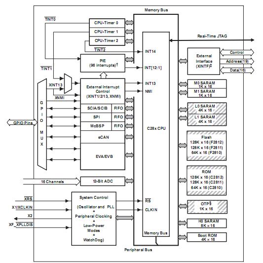
| Image | Part No | Mfg | Description |  |
Pricing (USD) |
Quantity | ||||||||||||
|---|---|---|---|---|---|---|---|---|---|---|---|---|---|---|---|---|---|---|
 |
 TMS320F2810PBKA |
 Texas Instruments |
 Digital Signal Processors & Controllers (DSP, DSC) 32-Bit Digital Sig Controller w/Flash |
 Data Sheet |

|
|
||||||||||||
| Image | Part No | Mfg | Description |  |
Pricing (USD) |
Quantity | ||||||||||||
 |
 TMS3112 |
 Other |
 |
 Data Sheet |
 Negotiable |
|
||||||||||||
 |
 TMS3121 |
 Other |
 |
 Data Sheet |
 Negotiable |
|
||||||||||||
 |
 TMS320 |
 Other |
 |
 Data Sheet |
 Negotiable |
|
||||||||||||
 |
 TMS32010 |
 Other |
 |
 Data Sheet |
 Negotiable |
|
||||||||||||
 |
 TMS320AV7110 |
 Other |
 |
 Data Sheet |
 Negotiable |
|
||||||||||||
 |
 TMS320BC51PQ100 |
 Texas Instruments |
 Digital Signal Processors & Controllers (DSP, DSC) TMS320C51PQ - 132QFP - 100MHZ/BOOT CODE |
 Data Sheet |
 Negotiable |
|
||||||||||||
 (China (Mainland))

